Literature/202311240722 compressive raman with spad arrays
- Source: [@gentner2023Compressive Raman microspectroscopy parallelized by single-photon avalanche diode arrays]
- Tags: #raman #compressive-raman #spectroscopy
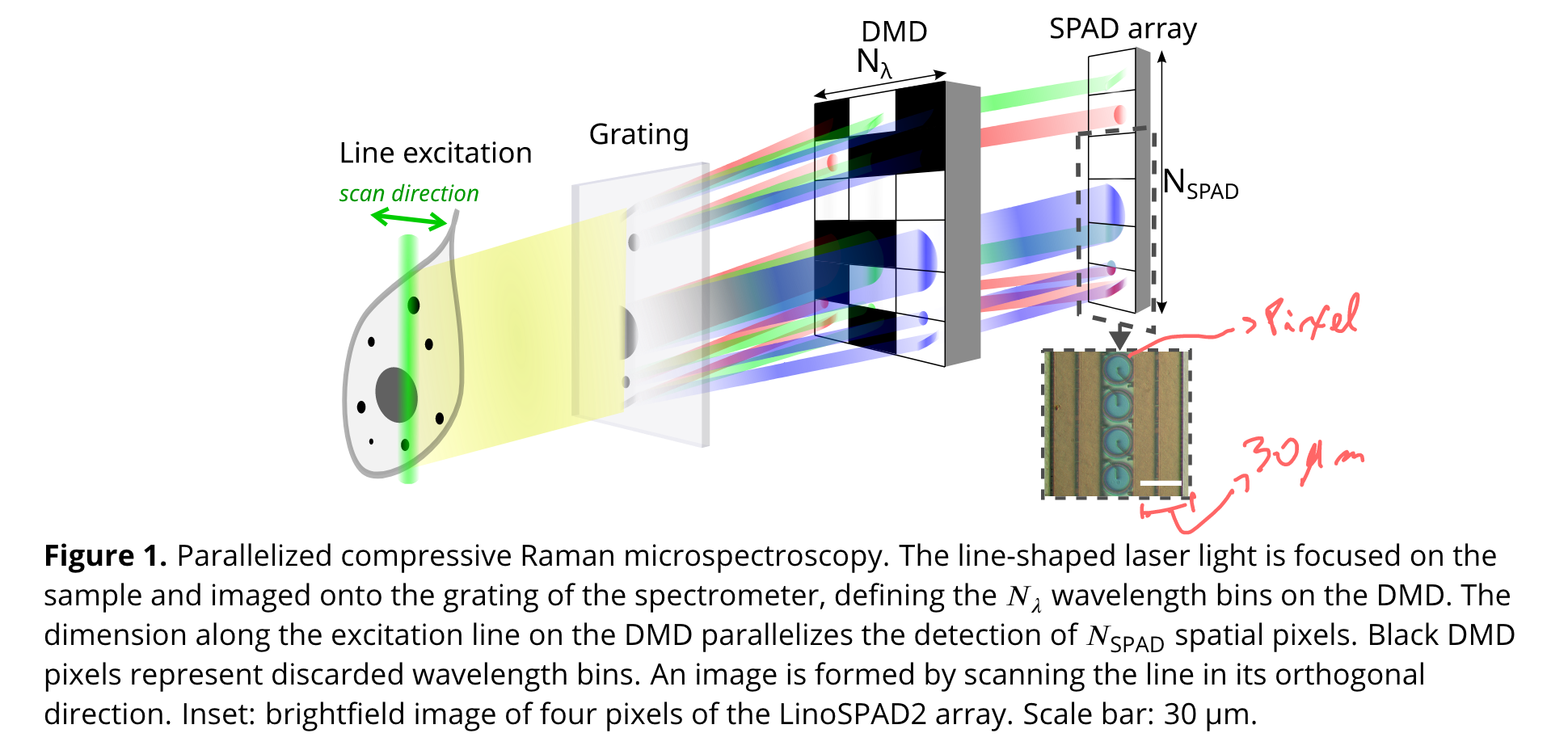
Compressive Raman is implemented on a SPAD array (nicknamed LinoSPAD2) using a DMD element and a line-scan microscope. This is very similar to what I had in mind with the light sheet spectrometry
The core idea behind is that instead of imaging the 2D spectrum on a CCD, a DMD is introduced in between. The DMD then selects the spectral regions of interest and only those are transmitted to the SPAD array. In a previous work ([@pandya2022Competing oxygen evolution reaction mechanisms revealed by high-speed compressive Raman imaging], 202311240735 Compressive Raman for Chemical Reactions) they used a single SPAD.
In a way this works like a configurable spectrometer, imaging exactly what needs to be imaged to distinguish elements.
It is interesting to note that a DMD is also a grating and it will add dispersion to the imaging system. The image below (the insets on the top) show how the PSF is changed at different wavelengths, degrading the overall spatial and spectral resolution (on the right there is pixel-crosstalk).
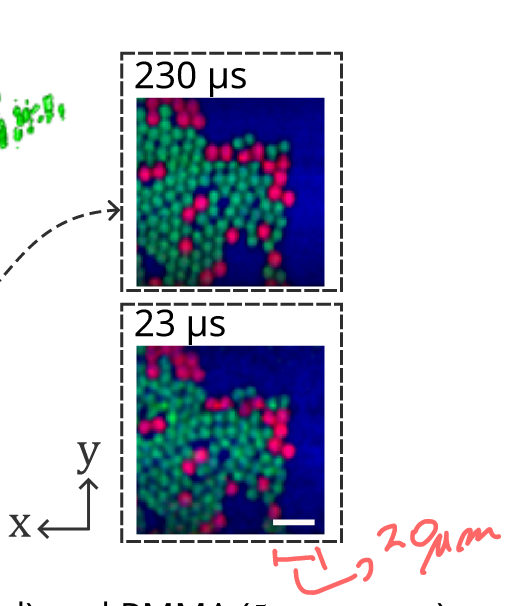
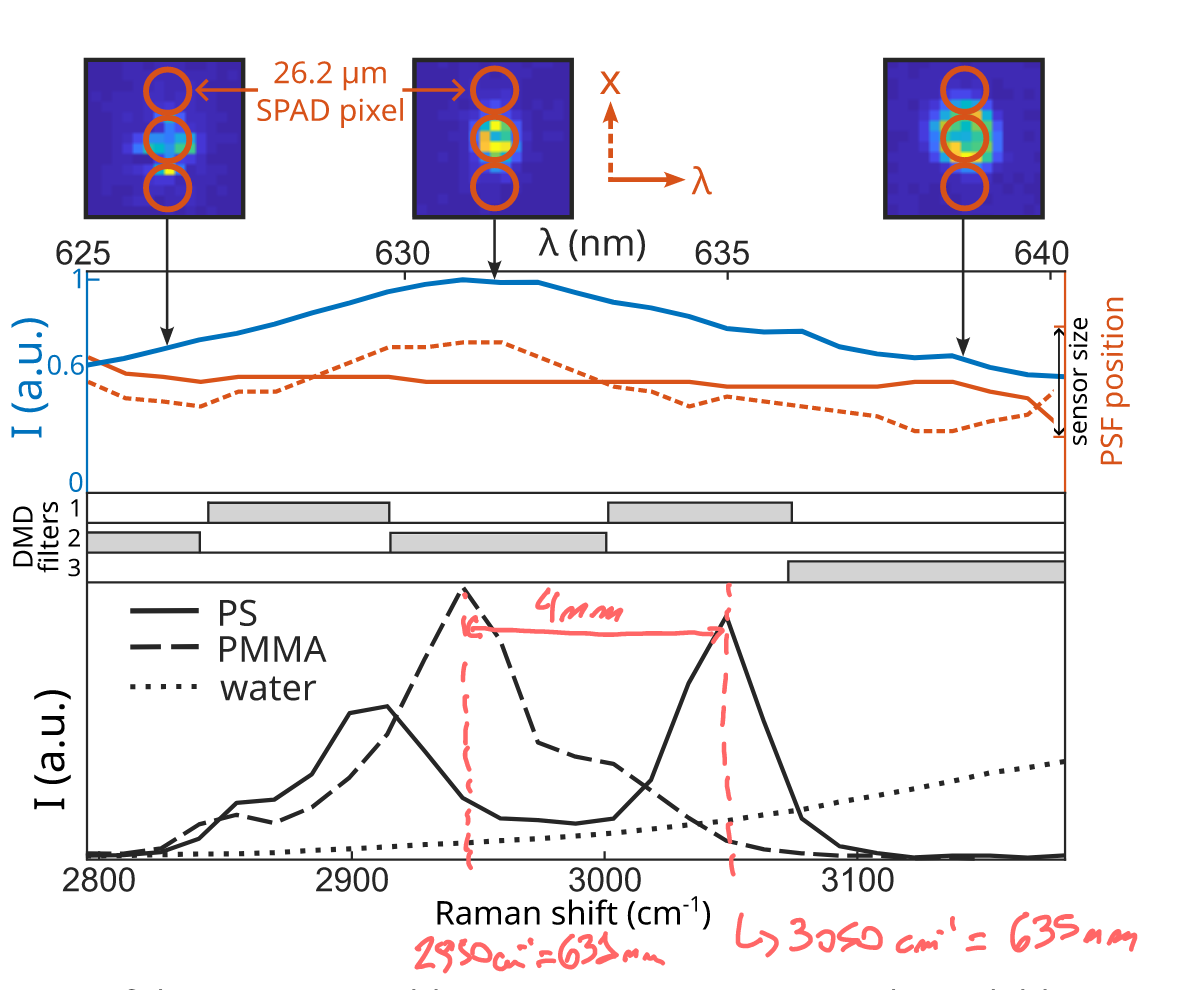 The system was used to identify PS and PMMA beads (of $6\mu m$ and $5\mu m$), and they are shown below:
Some numbers
- Pixel dwell-times ($\tau_{pdt}$) for a single detector are in the order of $1\mu s$.
- This paper achieves $\tau_{pdt}=23\mu s$, but as far as I understand, its over 128 pixels, hence an effective $\approx 5X$ improvement.
- Line-dwell times were between $10ms$ and $1ms$ (for the images with the beads)
Backlinks
These are the other notes that link to this one.
Comment